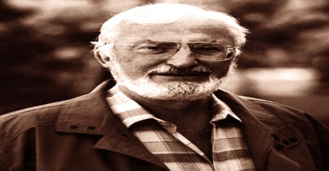
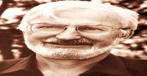
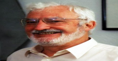
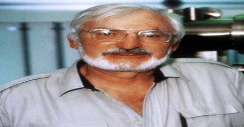
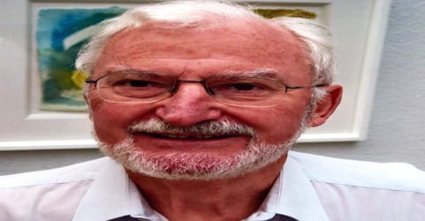
Biography of Heinrich Rohrer
Heinrich Rohrer – Swiss physicist.
Name: Heinrich Rohrer
Date of Birth: 6 June 1933
Place of Birth: Buchs, St. Gallen, Switzerland
Date of Death: 16 May 2013 (aged 79)
Place of Death: 16 May 2013 (aged 79)
Occupation: Physicist
Father: Hans Heinrich Rohrer
Mother: Katharina Gantenbein
Spouse/Ex: Rose-Marie Egger
Children: Doris Rohrer, Ellen Rohrer
Early Life
A Swiss physicist who, with Gerd Binnig, received half of the 1986 Nobel Prize for Physics for their joint invention of the scanning tunneling microscope, Heinrich Rohrer was born on June 6, 1933, in Buchs, Switzerland, to Hans Heinrich Roher and Katharina (Ganpenbein) Rohrer. Rohrer spent most of his career at the IBM Research Laboratories in Switzerland, where he conducted his most significant research. His other research interests included superconductivity, multicritical phenomena, and nanotechnology.
His participation in designing and building the Scanning Tunneling Microscope, an instrument so sensitive that it distinguishes individual atoms, earned him a share of the Nobel Prize in Physics in 1986. Though he received international acclaim for his career in physics, it was actually by chance that he ventured into the scientific field. As a young boy, he was more inclined towards the classical languages and it was only as a college student that he recognized his calling to be a physicist. After completing his education, he spent the majority of his career at IBM due to its flexibility and conducted most of his research there. He also dabbled in superconductivity, multi-critical phenomena, and nanotechnology. Rohrer believed that the world should be ready to exploit the new possibilities nanotechnology offers. A friendly man with a witty personality, he was a model physicist who was not only intelligent but also kind. He was a family man who cherished quality time with his wife and children. Even after his retirement, he continued to accept invitations for research projects in various universities across the globe. The many honors and awards he received during his lifetime are a small testament to a man who revolutionized the world of science.
Childhood, Family and Educational Life
Heinrich Rohrer was born half an hour later than his twin sister on June 6, 1933, in Buchs, St. Gallen, Switzerland. He was the third of three children born to Katharina Gantenbein and Hans Heinrich Rohrer. His father was a distributor of manufactured goods.
Rohrer recalled his childhood as being relatively carefree, with play, farm work, and schooling occupying much of his time. In 1939, when he was 13 years old, Rohrer’s family moved from the country to the large city of Zurich, a move that changed their lifestyle.
Being exposed to the country life, Rohrer was inclined towards classical languages and natural sciences. In 1951, he was enrolled at the Swiss Federal Institute of Technology (ETH) and he started favoring Physics. At ETH, he was taught by notable Professors G. Busch, Wolfgang Pauli, and Paul Scherrer. He earned his B.S. in 1955. Four years later, in 1955, Rohrer began working on his Ph.D. in experimental physics. He was entrusted with measuring the length changes of superconductors at the magnetic field-induced superconducting transition. Rohrer conducted his research after midnight because the mechanical transducers were sensitive to vibrations. In 1960, he received his Ph.D.
Personal Life
Heinrich Rohrer married Rose-Marie Egger in the summer of 1961. She was a supportive and stabilizing influence in his life. They had two daughters, namely, Doris Rohrer and Ellen Rohrer.
Quite an outdoorsy man, Rohrer went on a four-month camping trip through the USA in 1963. During his sabbatical at Santa Barbara, he took his family on two extended camping trips and showed them the States from coast to coast.
Career and Works
Heinrich Rohrer’s studies were interrupted by his military service in the Swiss mountain infantry. In 1961, he married Rose-Marie Egger. Their honeymoon trip to the United States included a stint doing research on thermal conductivity of type-II superconductors and metals with Bernie Serin at Rutgers University in New Jersey.
Following a four-month camping trip through the United States, Rohrer returned to Switzerland in 1963. In the summer of that year, Ambros Speiser, director of the newly founded IBM Research Laboratory in Ruschlikon, Switzerland, offered Rohrer a position at the company as a research staff assistant. Encouraged to accept this position by his professor Bruno Luthi, Rohrer joined IBM in December of 1963. His research efforts interests included Kondo systems, phase transitions, multicritical phenomena, scanning tunneling microscopy and, most recently, nanomechanics.
At IBM, Rohrer mainly worked on Kondo systems with magnetoresistance in pulsed magnetic fields for two years and later shifted his interest to magnetic phase diagrams. This led to his entry into the field of critical phenomena. He was encouraged by K. Alex Müller to focus on the bicritical and tetracritical behavior and finally on the random-field problem.
In 1974, Rohrer spent a sabbatical year at the University of California in Santa Barbara, California studying nuclear magnetic resonance with Vince Jaccarino and Alan King. His interest in complex atomic structures of surface materials brought him and Gerd Binnig together in 1978. Frustrated by the limits of the tools available, they decided to develop a spectroscopic probe that led to the design of the ‘Scanning Tunneling Microscope’. They submitted their patent in 1979.
Binnig joined the laboratory in 1978, and it was there that the two men designed and built the first scanning tunneling microscope. This instrument is equipped with a tiny tungsten probe whose tip, only about one or two atoms wide, is brought to within five or ten atoms’ distance of the surface of a conducting or semiconducting material. (An atom is equal to about one angstrom, or one ten-billionth of a meter.) When the electric potential of the tip is made to differ by a few volts from that of the surface, quantum mechanical effects cause a measurable electric current to cross the gap. The strength of this current is extremely sensitive to the distance between the probe and the surface, and, as the probe’s tip scans the surface, it can be kept a fixed distance away by raising and lowering it so as to hold the current constant. A record of the elevation of the probe is a topographical map of the surface under study, on which the contour intervals are so small that the individual atoms making up the surface are clearly recognizable.
Rohrer and Binnig tested their device in 1981 and continued to add refinements. In 1986, he and Binnig shared half of the prize of the Nobel Prize in Physics for their development of the Scanning Tunneling Microscope. This invention opened new doors in nanotechnology.
Rohrer was appointed IBM Fellow in 1986 and led the physics department of the research lab from 1986 until 1988. K. Alex Muller, who won a share of the 1987 Nobel Prize in Physics for breakthroughs in the discovery of superconductivity in ceramic materials, had pioneered efforts in critical phenomena at IBM’s Ruschlikon laboratory, and he encouraged Rohrer in this new direction. Roher focused on the bicritical and tetracritical behavior and on the random-field problem. “These were most enjoyable years, during which so many patient colleagues taught me physics,” recalled Rohrer in his Nobel autobiography.
Rohrer dedicated his entire career at the IBM Research Laboratory because of the freedom given to pursue his interests and the intellectual cooperation he received. Rohrer remained involved with IBM throughout his career. “In all the years with IBM Research, I have especially appreciated the freedom to pursue the activities I found interesting, and greatly enjoyed the stimulus, collegial cooperation, frankness, and intellectual generosity of two scientific communities, namely, in superconductivity and critical phenomena,” Rohrer wrote in his Nobel autobiography.
Rohrer retired from IBM in 1997. After his retirement, he accepted research appointments at the ‘Consejo Superior de Investigaciones Científicas’ in Madrid, Spain, and at ‘Riken University’ and ‘Tohoku University’ in Japan.
Rohrer believes the world should be ready to exploit the new possibilities nanotechnology represents. In addition, he feels that devices like the scanning tunneling microscope would be useful in addressing one of the biggest challenges of nanoscience and nanotechnology: improving the interface between the macroscopic world of traditional manufacturing and the “nano” world. The scanning tunneling microscope could help create such an interface and thus become one of the major tools of nanotechnology. Along with its imaging capabilities, the microscope could be reconfigured to manipulate molecules and atoms, and it would enable researchers and product developers to observe what happens at the molecular level so that they could modify and manufacture items at the nano level.
Awards and Honor
Heinrich Rohrer was the recipient of a number of awards, many of which were shared with his colleague and fellow researcher Gerd Binnig. In 1984, Rohrer was co-awarded the EPS Europhysics Prize and King Faisal Prize.
Along with Gerd Binnig and Ernst Ruska, Rohrer was awarded the Nobel Prize in Physics’ in 1986 for their design of the Scanning Tunneling Microscope. Ernst Ruska received half of the prize and the other half was shared by Binnig and himself.
In 1994, Rohrer was inducted into the ‘National Inventors Hall of Fame’. He is one of 532 inductees to be bestowed this honor.
Death and Legacy
Heinrich Rohrer died of natural causes on 16 May 2013 at his home in Wollerau, Switzerland, aged 79.
Heinrich Rohrer was one of the primary designers of the Scanning Tunneling Microscope (STM). It was an l invention that allowed for imaging surfaces at the atomic level. Many practical applications of the STM include better lithography, atomic disposition of metals which can later be used as nanodevices, rotation of individual bonds within single molecules, and many more.
The ‘Binnig and Rohrer Nanotechnology Center’ in Rüschlikon is dedicated to the team that built the STM.
Information Source: