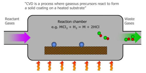
Chemical vapour deposition (CVD) is a coating process that uses thermally induced chemical reactions at the surface of a heated substrate, with reagents supplied in gaseous form. It is a vacuum deposition method used to produce high quality, high-performance, solid materials. CVD is a widely used technique to make 2D nanomaterials and thin films on solid substrates. The process is often used in the semiconductor industry to produce thin films. CVG reactors must be designed to control film parameters such as film thickness, crystal structure, surface morphology, the composition of the film, etc.
In typical CVD, the wafer (substrate) is exposed to one or more volatile precursors, which react and/or decompose on the substrate surface to produce the desired deposit. In this technique, the precursors, gas or vapor, can react or decompose on the preselected substrate at high temperature and vacuum in a chamber. Frequently, volatile by-products are also produced, which are removed by gas flow through the reaction chamber. CVD is a parent to a family of processes whereby a solid material is deposited from vapor by a chemical reaction occurring on or in the vicinity of a normally heated substrate surface.
Microfabrication processes widely use CVD to deposit materials in various forms, including – monocrystalline, polycrystalline, amorphous, and epitaxial. These materials include – silicon, carbon, fluorocarbons, filaments, tungsten, titanium nitride, and various high-k dielectrics. A characteristic feature of the CVD technique is its excellent throwing power, enabling the production of coatings of uniform thickness and properties with a low porosity even on substrates of complicated shape.
Uses
CVD is commonly used to deposit conformal films and augment substrate surfaces in ways that more traditional surface modification techniques are not capable of. The simplest CVD process involves the pyrolytic decomposition of a gaseous compound on the substrate to provide a coating of a solid reaction product. CVD is extremely useful in the process of atomic layer deposition at depositing extremely thin layers of material. A key advantage of the CVD process lies in the fact that the reactants used are gases, thereby taking advantage of the many characteristics of gases.
A variety of applications for such films exist. Gallium arsenide is used in some integrated circuits (ICs) and photovoltaic devices. Amorphous polysilicon is used in photovoltaic devices. Certain carbides and nitrides confer wear-resistance. The CVD of metal-organic frameworks, a class of crystalline nanoporous materials, has recently been demonstrated. CVD offers many advantages over other deposition processes. These include a wide range of coating materials based on metals, alloys, and ceramics.