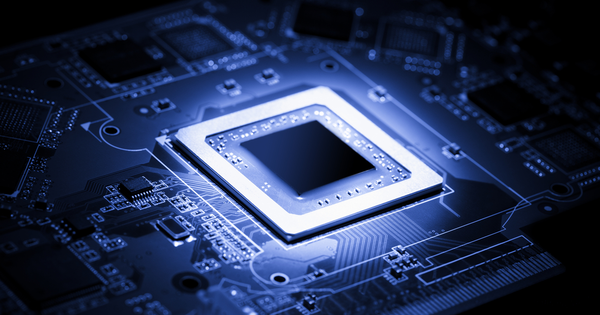
Our current chip technology is largely silicon-based. A trace amount of germanium is used in very specific components. However, there are several compelling reasons to use higher germanium contents in the future: In terms of energy efficiency and achievable clock frequencies, the compound semiconductor silicon-germanium has significant advantages over today’s silicon technology.
The main challenge here is to reliably establish contacts between metal and semiconductor on a nanoscale. With a high proportion of germanium, this is much more difficult than with silicon. The TU Wien team, in collaboration with research teams from Linz and Thun (Switzerland), has now demonstrated that this problem can be solved – with contacts made of extremely high-quality crystalline aluminum and a sophisticated silicon germanium layer system. This enables a variety of intriguing contact properties, particularly for optoelectronic and quantum components.
The problem with oxygen
“Every semiconductor layer is automatically contaminated in conventional processes; this simply cannot be prevented at the atomic level,” says Masiar Sistani of TU Wien’s Institute for Solid State Electronics. First and foremost, oxygen atoms accumulate rapidly on the surface of the materials, forming an oxide layer.
Our experiments show that these contact points can be produced in a reliable and easily reproducible manner. The technological systems required to do this are already in use in the chip industry today.
Walter Weber
This is not an issue with silicon because it always forms the same type of oxide. “With germanium, however, things are much more complicated,” Masiar Sistani explains. “In this case, a wide variety of oxides can form. However, this means that different nanoelectronic devices can have very different surface compositions and, as a result, different electronic properties.”
If you now want to connect a metallic contact to these components, you have a problem: Even if you try very hard to produce all these components in exactly the same way, there are still inevitably massive differences — and that makes the material complex to handle for use in the semiconductor industry.
“Reproducibility is a big problem,” says Prof. Walter Weber, the head of the Institute for Solid State Electronics, TU Wien. “If you use germanium-rich silicon germanium, you can’t be sure that the electronic component, after you’ve put contacts on it, will really have the characteristics you need.” As a result, this material is only used to a limited extent in chip production.
That is a pity, because silicon germanium would have decisive advantages: “The charge carrier concentration is higher, especially positive charge carriers, the so-called “holes,” can move much more efficiently in this material than in silicon. The material would therefore allow much higher clock frequencies with increased energy efficiency than our current silicon chips,” says Lukas Wind, a doctoral student in Walter Weber’s research group.
The “perfect” interface
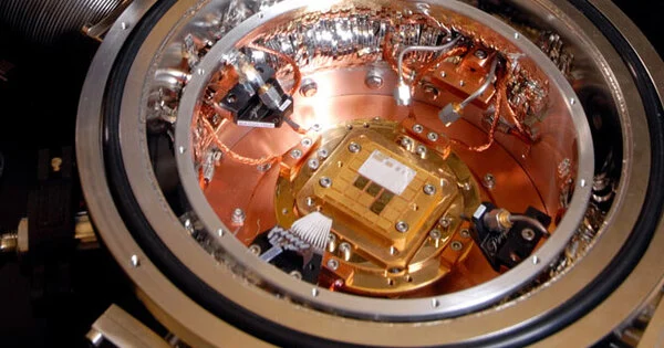
However, the research team has now demonstrated how the problem can be solved: On an atomic scale, they discovered a way to create perfect interfaces between aluminum contacts and silicon germanium components. In the first step, a layer system with a thin silicon layer and the actual material from which the electronic components will be made (silicon-germanium) is created.
A contact between the aluminium and the silicon can now be formed by heating the structure in a controlled manner: At around 500 degrees Celsius, distinct diffusion occurs, allowing atoms to leave their position and begin to migrate. Silicon and germanium atoms move quickly into the aluminium contact, and aluminium fills the void.
“The diffusion dynamics in the layer system used thus create an interface between aluminium and the silicon germanium with an extremely thin silicon layer in between,” explains Masiar Sistani. Through this manufacturing process, oxygen atoms never have the opportunity to get to this atomically sharp and highly pure interface.
“Our experiments show that these contact points can be produced in a reliable and easily reproducible manner,” says Walter Weber. “The technological systems required to do this are already in use in the chip industry today.” So this isn’t just a laboratory experiment, but a process that could be used in the chip industry relatively soon.
The presented manufacturing process has the distinct advantage of producing high-quality contacts regardless of silicon-germanium composition. “We are convinced that the presented abrupt, robust, and reliable metal-semiconductor contacts are highly interesting for a variety of new nanoelectronic, optoelectronic, and quantum devices,” says Walter Weber.