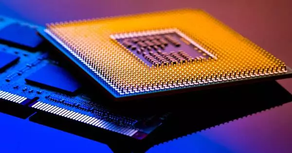
Semiconductor device fabrication refers to the process of producing semiconductor devices, which are typically integrated circuits (ICs) such as computer processors, microcontrollers, and memory chips (such as NAND flash and DRAM) found in everyday electrical and electronic devices. It refers to the manufacturing of integrated circuits (ICs) and other semiconductor devices. It entails a series of steps that convert raw materials into finished devices that perform specific functions.
It is a multi-step photolithographic and physio-chemical process (with steps such as thermal oxidation, thin-film deposition, ion-implantation, and etching) that gradually creates electronic circuits on a wafer made of pure single-crystal semiconducting material. Silicon is almost always used, but for specialized applications, various compound semiconductors are used.
The fabrication process is carried out in highly specialized semiconductor fabrication plants, also known as foundries or “fabs,” with the “clean room” serving as the central component. Fabrication of more advanced semiconductor devices, such as modern 14/10/7 nm nodes, can take up to 15 weeks, with the industry average being 11-13 weeks.
Here is a general overview of the semiconductor device fabrication process:
- Design and Layout: The process begins with the design of the semiconductor device, including its architecture, functionality, and circuit layout. Computer-aided design (CAD) tools are often used to create the layout.
- Wafer Preparation: Silicon wafers are the starting material for semiconductor fabrication. The wafers are typically made from highly pure single-crystal silicon. They undergo various cleaning and polishing steps to ensure their surface is smooth and free from contaminants.
- Photolithography: This step involves creating patterns on the wafer surface using light-sensitive materials called photoresists. The wafer is coated with a photoresist, and then a mask or reticle, containing the desired pattern, is used to expose the resist to ultraviolet light. This process transfers the pattern onto the wafer.
- Etching: Etching removes material from the wafer to create the desired circuit patterns. There are two main types of etching: wet etching and dry etching. Wet etching involves immersing the wafer in a chemical solution that selectively removes the exposed material. Dry etching uses plasma or reactive gases to etch the wafer surface.
- Doping: The process of introducing impurities into specific regions of a semiconductor material to modify its electrical properties is known as doping. Doping materials such as boron or phosphorus are used to create n-type (negative) or p-type (positive) regions, which are then used to form transistors, diodes, and other components.
- Deposition: Deposition is the process of depositing thin layers of material onto the surface of a wafer. This can be accomplished through the use of techniques such as chemical vapor deposition (CVD) or physical vapor deposition (PVD). Depending on the device requirements, the deposited materials may include metals, oxides, or polymers.
- Metallization: Metal layers are added to the wafer to create interconnections between the various components. Sputtering or electroplating techniques are used to pattern and deposit the metal layers. These metal layers serve as the electrical pathways that allow signals to pass through the device.
Following the completion of wafer fabrication, the individual chips are separated and packaged into their final form. The chips are packaged by encapsulating them in protective materials and connecting them to external leads. Following packaging, the devices are subjected to extensive testing to ensure functionality and quality.
To improve yield (the percentage of microchips that function correctly in a wafer), production in advanced fabrication facilities is completely automated and carried out in a hermetically sealed nitrogen environment, with automated material handling systems handling wafer transport from machine to machine. FOUPs, or special sealed plastic boxes, are used to transport wafers.
Internal nitrogen atmosphere is present in all machinery and FOUPs. In the cleanroom, the insides of the processing equipment and FOUPs are kept cleaner than the surrounding air. This internal environment is referred to as a mini-environment. Fabrication plants require large amounts of liquid nitrogen to maintain the atmosphere inside production machinery and nitrogen-purged FOUPs.