Engineers from Vanderbilt and Penn State have developed a new method for designing and fabricating thin-film infrared light sources with near-arbitrary spectral output driven by heat, as well as a machine learning methodology called inverse design, which reduced the optimization time for these devices from weeks or months on a multi-core computer to a few minutes on a consumer-grade desktop.
The capacity to create low-cost, high-efficiency designer infrared light sources has the potential to transform molecular sensing technology. Free-space communications, infrared beacons for search and rescue, and molecular sensors for monitoring industrial gases, pollutants, and poisons are among the other uses.
The strategy, which was published in Nature Materials today, relies on basic thin-film deposition, one of the most well-established nanofabrication processes, and is supported by major developments in materials and machine learning. Broadband thermal radiation is produced by standard thermal emitters, such as incandescent light bulbs, limiting its utility to basic applications.
Lasers and light-emitting diodes, on the other hand, provide the narrow frequency emission required for many applications but are inefficient and/or costly. This has led to the development of wavelength-selective thermal emitters, which have the restricted bandwidth of a laser or LED but the simplicity of a thermal emitter.
The combination of the cadmium oxide material tunability with the fast optimization of aperiodic distributed Bragg reflectors offers the potential to design infrared light sources with user-defined output spectra. While these have immediate potential in chemical sensing, these also exhibit significant promise in a variety of other applications ranging for environmental and remoted sensing, spectroscopy, and infrared signaling and communications.
Joshua Caldwell
Most heat emitters with user-defined output spectrum have, however, needed patterned nanostructures manufactured with high-cost, low-throughput technologies to date. The study team, lead by Joshua Caldwell, associate professor of mechanical engineering at Vanderbilt, and Jon-Paul Maria, professor of materials science and engineering at Penn State, set out to solve long-standing problems and improve the technique.
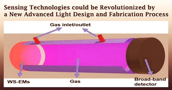
Their method takes advantage of the semiconductor cadmium oxide’s broad spectrum tunability in combination with a distributed Bragg reflector, a one-dimensional photonic crystal produced using alternating layers of dielectrics.
The interactions between these numerous layers of materials produce a so-called “Tamm-polariton,” in which the device’s emission wavelength is determined by the interactions between these layers. Until date, such devices could only provide a single wavelength output.
However, matching the absorption spectra of most molecules necessitates the creation of several resonances at different frequencies with user-controlled wavelength, line width, and intensity. Material design has proved difficult and time-consuming computationally.
The new technique has to dramatically reduce design time since sophisticated applications demand functioning at various resonances. For example, a typical gadget could have tens to hundreds of designable characteristics, resulting in high customization needs and unreasonable calculation times.
For example, if nine parameters are optimized individually, with 10 points each parameter sampled, the simulations would take 15 days assuming 100 simulations per second. However, when more factors are included, the time becomes increasingly longer. Three and 31 years, respectively, would be required for 11 and 12 parameters.
Mingze He, the paper’s primary author, introduced an inverse design technique that computes an optimal structure in minutes on a consumer-grade workstation to address this problem. Additionally, this code may be able to match the required emission wavelength, linewidth, and amplitude of numerous resonances over an arbitrary spectral bandwidth at the same time.
Another stumbling block was finding a semiconductor material with a wide dynamic range of electron densities. The team employed doped semiconductor material, which was produced by Maria’s Penn State research team and enables for the purposeful creation of optical features.
“This allows the fabrication of advanced mid-infrared light sources at wafer-scale with very low cost and minimal fabrication steps,” He said.
This phase of the experiment was carried out with Penn State colleagues, while He and J. Ryan Nolen, a recent Caldwell group graduate, characterized the devices. The two groups effectively proved the capabilities of inversely constructed infrared light sources when they worked together.
“The combination of the cadmium oxide material tunability with the fast optimization of aperiodic distributed Bragg reflectors offers the potential to design infrared light sources with user-defined output spectra. While these have immediate potential in chemical sensing, these also exhibit significant promise in a variety of other applications ranging for environmental and remoted sensing, spectroscopy, and infrared signaling and communications.” Caldwell said.
The design method has been open-sourced by the Caldwell group, and it may be downloaded from the Nature Materials and the Caldwell Infrared Nanophotonic Materials and Devices laboratory websites.
“Deterministic inverse design of Tamm plasmon thermal emitters with multi-resonant control,” their research was published on October 21. The National Science Foundation, the Office of Naval Research, the Army Research Office, the National Defense Science and Engineering Graduate Fellowship, and the Office of Naval Research were among the funding sources.