Quantum effects in superconductors have the potential to give semiconductor technology a new spin. Researchers at the Paul Scherrer Institute PSI and Cornell University in New York State have discovered a composite material that could integrate quantum devices into semiconductor technology, significantly increasing the power of electronic components. They published their findings in the journal Science Advances today.
Our current electronic infrastructure is primarily comprised of semiconductors. This class of materials first appeared in the mid-twentieth century and has steadily improved since then. Currently, the most significant challenges in semiconductor electronics include further advancements that would increase data transmission bandwidth, energy efficiency, and information security. Exploiting quantum effects will almost certainly be a game-changer.
The quantum effects that can occur in superconducting materials are particularly interesting. Superconductors are materials that lose their electrical resistance when cooled below a certain temperature. The use of quantum effects in superconductors has already been demonstrated in the first quantum computers.
We are looking into heterojunctions, which are structures made of two different types of materials, to find possible successors to today’s semiconductor electronics. It has long been known that you need to choose materials with very similar crystal structures for this, so that there is no tension in the crystal lattice at the contact surface.
John Wright
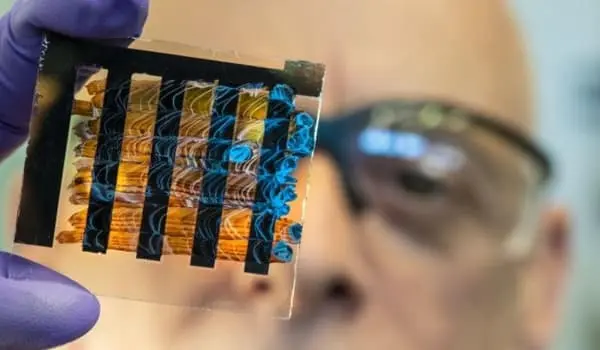
Some researchers, including a group at Cornell University, are looking into so-called heterojunctions, which are structures made of two different types of materials, to find possible successors to today’s semiconductor electronics. They are specifically interested in layered systems of superconducting and semiconducting materials. “It has long been known that you need to choose materials with very similar crystal structures for this, so that there is no tension in the crystal lattice at the contact surface,” says John Wright, who created the heterojunctions for the new study at Cornell University.
In this regard, the superconductor niobium nitride (NbN) and the semiconductor gallium nitride are both appropriate materials (GaN). The latter already plays an important role in semiconductor electronics and is thus well researched. Until now, however, it was unclear how electrons behaved at the contact interface of these two materials – and whether electrons from the semiconductor could interfere with superconductivity and thus obliterate the quantum effects.
“When I came across the Cornell group’s research, I knew: here at PSI, we can find the answer to this fundamental question with our spectroscopic methods at the ADRESS beamline,” says Vladimir Strocov, PSI researcher at the Synchrotron Light Source SLS.
This is how the two groups came to collaborate. In their experiments, they eventually found that the electrons in both materials “keep to themselves.” No unwanted interaction that could potentially spoil the quantum effects takes place.
Synchrotron light reveals the electronic structures
The PSI researchers used an established method at the SLS’s ADRESS beamline: angle-resolved photoelectron spectroscopy using soft X-rays, or SX-ARPES for short. “We can visualize the collective motion of the electrons in the material using this method,” explains Tianlun Yu, a postdoctoral researcher in Vladimir Strocov’s team who carried out the measurements on the NbN/GaN heterostructure. Yu is the new publication’s first author, along with Wright.
The SX-ARPES method generates a map with spatial coordinates that show the energy of electrons in one direction and something resembling their velocity in the other; more precisely, their momentum. “The electronic states appear as bright bands on the map in this representation,” Yu explains. The key research finding: the respective “bands” are clearly separated from each other at the material boundary between niobium nitride NbN and gallium nitride GaN. This indicates to the researchers that the electrons remain in their original material and do not interact with electrons in neighboring materials.
“The most important conclusion for us is that the superconductivity in the niobium nitride remains unaffected, even if this is placed atom by atom to match a layer of gallium nitride,” Vladimir Strocov says. “We were able to provide another piece of the puzzle that confirms: This layer system could actually lend itself to a new type of semiconductor electronics that embeds and exploits the quantum effects that occur in superconductors.”