Engineers developed an infrared imager that could be used to see through smog and fog, easily locate blood vessels on a patient, and inspect the quality of electronic boards through silicon wafers. It is also slimmer, more compact, and less expensive to manufacture than comparable technologies.
Seeing through the haze and fog. Mapping a person’s blood vessels while monitoring their heart rate – all without touching their skin. Examining the quality and composition of electronic boards by looking through silicon wafers. These are just a few of the features of a new infrared imager developed by a team of researchers led by electrical engineers at the University of California, San Diego.
The imager detects a portion of the infrared spectrum known as shortwave infrared light (wavelengths ranging from 1000 to 1400 nanometers), which is just outside the visible spectrum (400 to 700 nanometers). Thermal imaging, which detects much longer infrared wavelengths emitted by the body, is not to be confused with shortwave infrared imaging.
An infrared imager developed by engineers could be used to see through smog and fog; easily locate blood vessels on a patient, and see-through silicon wafers to inspect the quality of electronic boards.
The imager works by illuminating an object or area of interest with shortwave infrared light and then converting the low energy infrared light that is reflected back to the device into shorter, higher-energy wavelengths that the human eye can see. “It makes invisible light visible,” said Tina Ng, an electrical and computer engineering professor at the University of California, San Diego Jacobs School of Engineering.
While infrared imaging technology has been around for decades, most systems are expensive, bulky, and complex, necessitating the use of a separate camera and display. Inorganic semiconductors, which are expensive, rigid, and contain toxic elements such as arsenic and lead, are also commonly used.
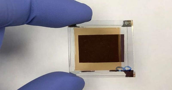
These issues are overcome by the infrared imager developed by Ng’s team. It combines sensors and a display into a single thin device, making it small and easy to use. Because it is made of organic semiconductors, it is low-cost, flexible, and safe for use in biomedical applications. It also has higher image resolution than some inorganic counterparts.
The new imager, which was recently published in Advanced Functional Materials, provides additional benefits. It seems more of the shortwave infrared spectrum, from 1000 to 1400 nanometers, whereas existing similar systems typically see only below 1200 nanometers. It also has one of the largest infrared imager display sizes to date: 2 square centimeters. Furthermore, because the imager is made using thin-film processes, it is simple and inexpensive to scale up to make larger displays.
Energizing infrared photons to visible photons
The imager is made up of hundreds of nanometer-thin semiconducting layers stacked on top of one another. The imager’s key players are three of these layers, each made of a different organic polymer: a photodetector layer, an organic light-emitting diode (OLED) display layer, and an electron blocking layer in between.
Shortwave infrared light (low energy photons) is absorbed by the photodetector layer, which generates an electric current. This current is directed to the OLED display layer, where it is converted into a visible image (high-energy photons). The electron-blocking layer is an intermediate layer that prevents the OLED display layer from losing any current. This is what enables the device to produce a clearer image.
Upconversion is the process of converting low-energy photons to higher energy photons. The upconversion process in this case is unique in that it is electronic. “The benefit of this is that it allows direct infrared-to-visible conversion in a single thin and compact system,” said first author Ning Li, a postdoctoral researcher in Ng’s lab. “A detector array to collect data, a computer to process that data, and a separate screen to display that data are required in a typical IR imaging system where upconversion is not electronic. This is why most existing systems are cumbersome and costly.”
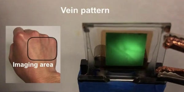
Another unique feature is that the imager can provide both optical and electronic readouts. “This makes it multifunctional,” Li explained. When the researchers shined an infrared light on the back of a subject’s hand, the imager provided a picture of the subject’s blood vessels while also recording the subject’s heart rate.
In addition, the researchers used an infrared imager to see through smog and a silicon wafer. In one experiment, they placed a photomask with the word “EXIT” on it in a small chamber filled with smog. In another, they hid a silicon wafer behind a photomask emblazoned with “UCSD.” Infrared light can pass through smog and silicon, allowing the imager to see the letters in these demonstrations. This could be useful for things like assisting autonomous vehicles to see in bad weather and inspecting silicon chips for flaws.