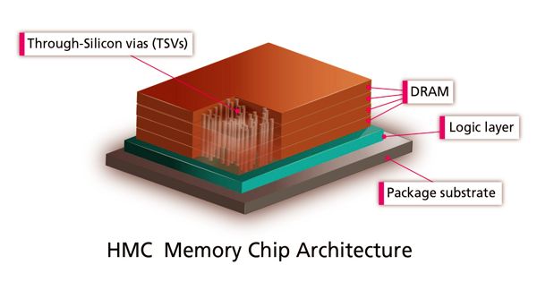
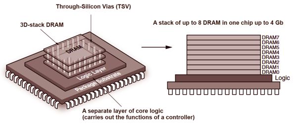
Hybrid Memory Cube (HMC) is a single package containing four DRAM die and one logic die, all stacked together using through-silicon via (TSV) technology. HMC is a high-performance RAM interface for through-silicon vias (TSV)-based stacked DRAM memory competing with the incompatible rival interface High Bandwidth Memory (HBM). HMCs consist of several layers connected by silicon. The upper layers are DRAM-memory crystals; the lower layer is a controller that controls the transfer of data.
The Hybrid Memory Cube is a three-dimensional DRAM architecture that improves latency, bandwidth, power, and density. Multiple DRAM layers are connected to a logic base layer to form a 3-D, high capacity, small footprint package.
HMC is used where speed and a small number of chips are necessary for the required amount of memory. Chips are available in capacities of 2 GB and 4 GB. Data is transmitted via serial interfaces at a speed of 15 Gbit/s per line; the total number of lines can be from 32 to 64.
Overview
Hybrid Memory Cube was co-developed by Samsung Electronics and Micron Technology in 2011, and announced by Micron in September 2011. It promised a 15 times speed improvement over DDR3. While DDR4 and DDR5 represent an evolution of the standard, HMC is a memory technology that could affect the fields of specialized high-performance computing and consumer electronics, such as tablets and graphics cards, where form factor is important as well as energy efficiency and throughput.
HMC chips can be combined into a consistent chain of up to eight pieces. The Hybrid Memory Cube Consortium (HMCC) is backed by several major technology companies including Samsung, Micron Technology, Open-Silicon, ARM, HP (since withdrawn), Microsoft (since withdrawn), Altera (acquired by Intel in late 2015), and Xilinx. Micron, while continuing to support HMCC, is discontinuing the HMC product in 2018 when it failed to achieve market adoption. Initially used in supercomputers and high-speed servers, HMC memory is expected to migrate to all types of computing devices.
HMC combines through-silicon vias (TSV) and microbumps to connect multiple (currently 4 to 8) dies of memory cell arrays on top of each other. The memory controller is integrated as a separate die. HMC consists of a single package containing multiple memory die and one logic die, stacked together using through-silicon via (TSV) technology. Within HMC, memory is organized into vaults. Each vault is functionally and operationally independent.
HMC uses standard DRAM cells but it has more data banks than classic DRAM memory of the same size. The HMC interface is incompatible with current DDRn (DDR2 or DDR3) and competing High Bandwidth Memory implementations.
Information Source: