Skin electronics are thin, flexible electronic devices that can be attached to the skin. While it may sound like something out of a science fiction movie, such devices are expected to serve as next-generation devices with a wide range of applications such as health monitoring, health diagnosis, virtual reality, and human-machine interface in the near future.
Skin electronics necessitate stretchable conductors with metal-like conductivity, high stretchability, ultrathin thickness, and ease of pattern ability, but achieving all of these characteristics at the same time is difficult. The researchers created a new float assembly method to create a nanomembrane that meets all of these requirements at the same time. The material’s exceptional properties are attributed to its unique cross-sectional structure, which consists of a monolayer of compactly assembled nanomaterials partially embedded in an ultrathin elastomer membrane.
As expected, creating such devices necessitates the use of soft and stretchable components that are mechanically compatible with human skin. An intrinsically stretchable conductor that transmits electrical signals between devices is a critical component of skin electronics. A stretchable conductor with ultrathin thickness, metal-like conductivity, high stretchability, and ease of patentability is required for reliable operation and high-quality performance. Despite extensive research, it has not yet been possible to create a material that possesses all of these properties at the same time, due to the fact that they frequently have trade-offs between them.
Skin electronics require stretchable conductors that satisfy metal-like conductivity, stretchability, and ease of pattern ability, but it is challenging to achieve these characteristics. Researchers developed a new float assembly method to fabricate a nanomembrane that satisfies all these requirements.
Researchers at the Institute for Basic Science (IBS) in Seoul, South Korea, led by professor HYEON Taeghwan and KIM Dae-Hyeong, unveiled a new method for fabricating a composite material in the form of a nanomembrane with all of the above-mentioned properties. Metal nanowires are tightly packed in a monolayer within an ultrathin rubber film to form the new composite material.
This novel material was created using a process developed by the team known as the “float assembly method.” The float assembly takes advantage of the Marangoni effect, which occurs when two liquid phases with different surface tensions come into contact with each other. When there is a gradient in surface tension, a Marangoni flow is generated away from the lower surface tension region and towards the higher surface tension region. Dropping a liquid with lower surface tension on the water surface lowers the surface tension locally, and the resulting Marangoni flow causes the dropped liquid to spread thinly across the water’s surface.
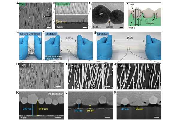
A three-step process is used to create the nanomembrane using a float assembly method. The first step is to drop a composite solution on the surface of the water, which is a mixture of metal nanowires, rubber dissolved in toluene, and ethanol. Because of its hydrophobic property, the toluene-rubber phase remains above the water, while the nanowires end up on the interface between the water and toluene phases.
The ethanol in the solution reacts with the water to lower the local surface tension, causing Marangoni flow to propagate outward and prevent the nanowires from aggregating. This forms a monolayer of nanomaterials at the interface of water and a very thin rubber/solvent film. The surfactant is then dropped in the second step, causing a second wave of Marangoni flow to compact the nanowires. Finally, in the third step, the toluene is evaporated, yielding a nanomembrane with a one-of-a-kind structure consisting of a highly compacted monolayer of nanowires partially embedded in an ultrathin rubber film.
Its unique structure enables efficient strain distribution in ultrathin rubber films, resulting in excellent physical properties such as stretchability of over 1,000% and a thickness of only 250 nm. The structure also allows for cold welding and bi-layer stacking of the nanomembranes, resulting in a metal-like conductivity of over 100,000 S/cm. Furthermore, the researchers demonstrated that the nanomembrane can be patterned using photolithography, a key technology used in the production of commercial semiconductor devices and advanced electronics. As a result, the nanomembrane is expected to serve as a new platform material for skin electronics.
The implications of this research could extend far beyond the development of skin electronics. While this study focused on a composite material made of silver nanowires within styrene-ethylene-butylene-styrene (SEBS) rubber, the float assembly method can also be used on magnetic nanomaterials and semiconducting nanomaterials, as well as other types of elastomers like TPU and SIS. As a result, the float assembly is expected to open up new research fields involving various types of nanomembranes with different functions.